

Pull to refresh
Logo
Applied Materials opens world's largest chip R&D center in Silicon Valley

Applied Materials opens world's largest chip R&D center in Silicon Valley

New Capabilities

Rival chipmakers will work side by side in a $5B facility to accelerate AI chip development

Yesterday: EPIC Center opens in Sunnyvale

Overview

Updated 2 hours ago

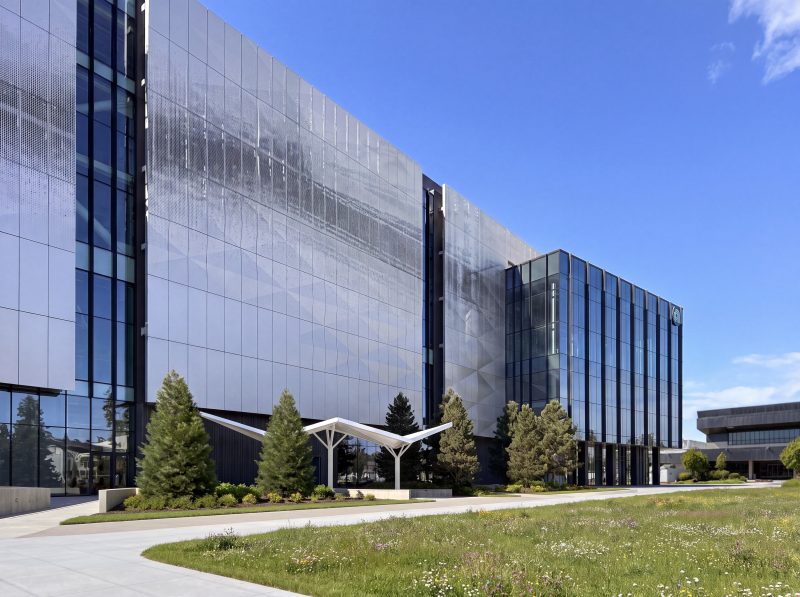
Applied Materials opened a $5 billion research complex in Sunnyvale, California, where the world's biggest chipmakers will work side by side on AI chip technology. The Equipment and Process Innovation and Commercialization (EPIC) Center is the largest facility ever built for collaborative semiconductor R&D.

The center collapses the traditional handoffs between materials research, equipment development, and process integration. TSMC, Intel, Samsung, Micron, and SK hynix will bring their own engineers and roadmaps into the building, working with Applied's scientists on the same wafers. The $5 billion figure is projected, not spent; Applied says spending will scale to that level as customer projects begin.

Why it matters

If EPIC works, AI chips reach production months faster, cutting the cost and risk of the industry's most expensive bottleneck.

Questions about this story

Free account needed to ask — your question is kept and asked for you right after sign-up. Answers are public.

No questions yet — be the first to ask.

Key Indicators

$5B
Projected capital investment
Expected to scale to this level as customer projects begin; first announced at $4B in 2023.
5
Founding chipmaker partners
TSMC, Intel, Samsung Electronics, Micron, and SK hynix.
600,000
Square feet of facility space
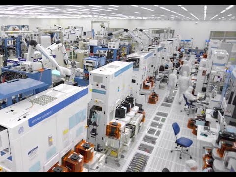
Includes nearly four acres of cleanroom space; took over six million construction hours to build.

Voices

Curated perspectives — historical figures and your fellow readers.

Ever wondered what historical figures would say about today's headlines?

Sign up to generate historical perspectives on this story.

People Involved

Organizations Involved

Timeline

May 2023 October 2026

3 events Latest: Yesterday
  1. EPIC Center opens in Sunnyvale

    Latest Opening

    Applied Materials unveils the $5 billion facility with founding partners TSMC, Intel, Samsung, Micron, and SK hynix.

  2. Intel and Applied Materials announce joint research

    Partnership

    Collaboration covers transistors, interconnects, and Foveros-based 3D packaging at EPIC and Intel's Hillsboro campus.

  3. Applied Materials announces EPIC Center

    Announcement

    Company plans up to $4 billion in capital spending over seven years for a collaborative chip R&D facility in Sunnyvale.

Scenarios

1

EPIC accelerates AI chip development

Likely Resolves by Oct 12, 2028

Discussed by: Applied Materials executives and industry analysts

Partners report measurable reductions in the time from research breakthrough to volume production. The collaborative model proves itself as chipmakers bring more programs into the facility and expand their commitments.

2

EPIC fails to deliver promised acceleration

Unlikely Resolves by Oct 12, 2028

Discussed by: Industry skeptics

The collaborative model produces few breakthroughs. Partners reduce their engagement, and the center becomes a costly showcase rather than a working lab. Applied faces writedowns or program delays.

3

EPIC model spreads across the industry

Possible Resolves by Oct 12, 2029

Discussed by: Industry observers

The collaborative model becomes the standard for semiconductor R&D. More companies join the EPIC ecosystem, and competitors build similar facilities to match.

Historical Context

2 moments from history that rhyme with this story — and how they unfolded.

1987-2015

SEMATECH (1987)

The U.S. government and 14 semiconductor companies formed SEMATECH, a consortium in Austin, Texas, to counter Japan's dominance in chip manufacturing. Member companies shared R&D costs and results in a common facility.

Then

SEMATECH helped U.S. chipmakers regain manufacturing leadership by the mid-1990s through shared process development.

Now

The consortium became a global model for pre-competitive collaboration and wound down its core operations in 2015.

Why this matters now

Like SEMATECH, EPIC brings rival companies into shared facilities to solve common manufacturing problems. The difference is that EPIC is run by a single equipment supplier rather than a government-backed consortium.

1984-present

IMEC (1984)

IMEC, founded in Leuven, Belgium, became the world's leading independent semiconductor research hub. Companies pay to access its cleanrooms and research programs, working on pre-competitive technology.

Then

IMEC's model of paid access to shared research facilities attracted most major chipmakers and equipment suppliers as members.

Now

The model became the industry standard for early-stage chip research, with IMEC remaining a central hub for advanced node development.

Why this matters now

EPIC borrows IMEC's collaborative model but focuses on later-stage development and commercialization, bringing equipment, materials, and process work into one facility owned by a single company.

Sources

(10)