

Pull to refresh
Logo
Silicon air-hole metasurface focuses ultraviolet light

Silicon air-hole metasurface focuses ultraviolet light

New Capabilities

University of Stuttgart researchers turn silicon's UV absorption into a flat mirror that focuses 325-nanometer light

Overview

Updated Yesterday

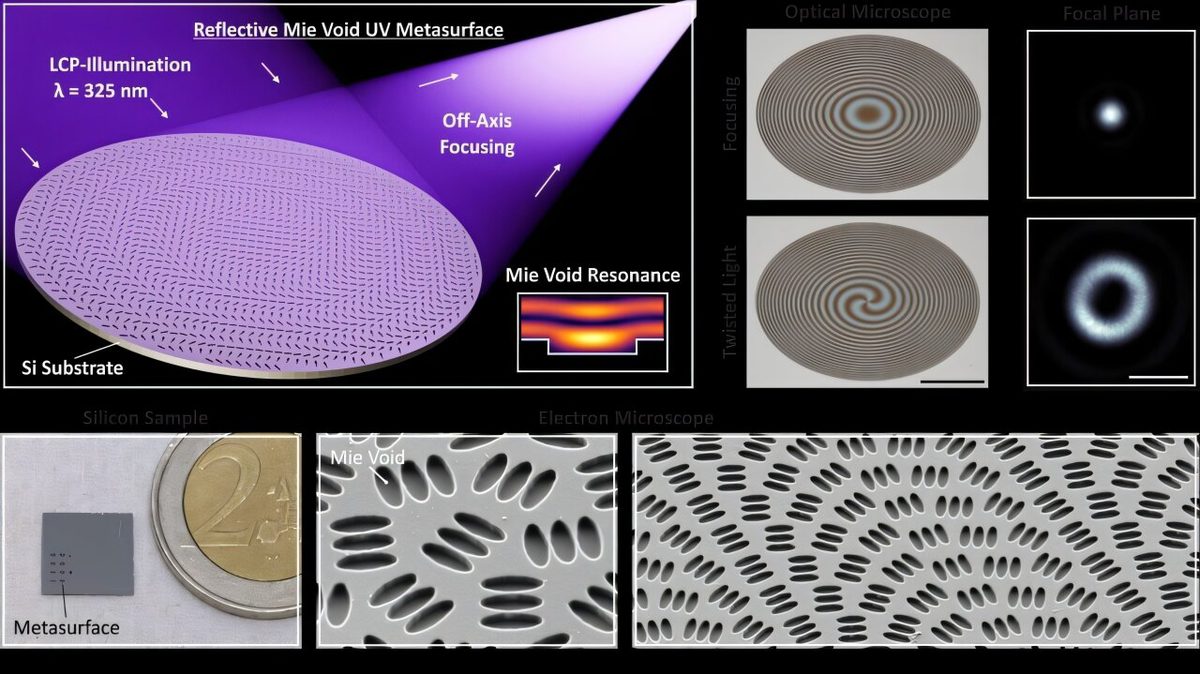
Silicon absorbs ultraviolet light, which is why UV optics usually depend on curved mirrors made from other materials. A University of Stuttgart team etched tiny air-filled cavities into silicon and used them to focus 325-nanometer light on a flat surface.

The device redirects a beam by 90 degrees and produces focal spots near the diffraction limit at numerical apertures up to 0.15. If the process scales, compact UV systems for imaging, spectroscopy and sensing could be built on standard semiconductor wafers.

Why it matters

Cheap, flat silicon optics could replace bulky curved mirrors in UV imaging, spectroscopy and sensing systems.

Questions about this story

Free account needed to ask — your question is kept and asked for you right after sign-up. Answers are public.

No questions yet — be the first to ask.

Key Indicators

325 nm
Operating wavelength
The ultraviolet wavelength the metasurface reflects and focuses.
~1 µm
Focal spot size
Smallest circular focal spot produced by the fabricated devices.
0.15
Numerical aperture
Spot size approached the diffraction limit up to this aperture.
90°
Beam redirection
Light arrives at 45 degrees and is turned and focused like an off-axis parabolic mirror.
1.25–5 mm
Focal length range
Focal lengths of the fabricated metasurfaces.

Voices

Curated perspectives — historical figures and your fellow readers.

Sign up to generate historical perspectives on this story.

People Involved

Organizations Involved

Timeline

January 2023 November 2026

3 events Latest: 2 days ago
  1. Results reported publicly

    Latest Publication

    Report describes 325-nanometer focusing, 1-micrometer spots and single-step fabrication.

  2. UV focusing metasurface paper published

    Research

    Advanced Photonics publishes the Stuttgart team's silicon air-void focusing mirror.

  3. Mie voids trap light in air

    Research

    Researchers show that tiny cavities in silicon can confine resonant light in air, down to 265 nanometers.

Scenarios

1

UV metasurfaces reach commercial sensing devices

Possible Resolves by End of 2028

Discussed by: Optics researchers and industry analysts following the paper

If established semiconductor fabrication can produce these metasurfaces at wafer scale, they could enter compact UV imaging, spectroscopy or biosensing equipment. The single-step lithography and etching process is the main cost argument. Adoption would depend on packaging and on whether device makers accept reflective rather than transmissive optics.

2

Approach extended to deep or vacuum UV

Uncertain Resolves by Q2 2029

Discussed by: The research team and photonics commentators

Because the mechanism tolerates and even benefits from material absorption, the team argues it can be pushed to shorter wavelengths. Success would require fabricating smaller voids and controlling the phase at those scales. The paper presents this as a prospect, not a demonstrated result.

3

Stays a lab demonstration

Possible Resolves by End of 2028

Discussed by: Cautious observers of academic metasurface research

Many metasurface results remain experimental because fabrication tolerances, efficiency and integration are hard to scale. If no commercial or shorter-wavelength follow-up appears, the 325-nanometer device remains a proof of concept.

Historical Context

2 moments from history that rhyme with this story — and how they unfolded.

January 2023

Dielectric Mie voids demonstrated (2023)

A Stuttgart-led team showed that air cavities milled into bulk silicon support resonant optical modes confined mainly in air. They observed resonant confinement down to 265 nanometers in the ultraviolet.

Then

Established Mie voids as a way to use high-index materials at wavelengths where they absorb.

Now

Provided the physical basis for the 2026 focusing metasurface and for UV color printing demonstrations.

Why this matters now

The new focusing mirror is a direct application of the void-confinement principle, scaled into a full wavefront-shaping surface.

2023

EUV metalens by vacuum guiding (2023)

Researchers at JILA and collaborators built a metalens from an array of holes in a thin silicon membrane that focused extreme-ultraviolet light near the diffraction limit by guiding it through vacuum.

Then

Demonstrated a 10-millimeter focal length lens with numerical apertures up to 0.05 at roughly 50 nanometers.

Now

Opened transmissive optics to a spectral range where most materials absorb strongly.

Why this matters now

It uses the same counterintuitive trick: holes in silicon manipulate light in a regime where solid silicon would absorb it.

Sources

(5)