Anchor

Samsung stacks memory directly on AI accelerators with zHBM prototype
New CapabilitiesThe 3D architecture removes the interposer, targeting 8x performance and 3x power efficiency over HBM5
3 days ago: Samsung debuts zHBM prototypeNew here? Follow stories to track developments over time. Create a free account to get updates when stories you care about change.
Overview
Updated 1 hour agoSamsung has shown a working prototype of zHBM, a memory architecture that stacks high-bandwidth memory directly on top of AI accelerators. The design removes the interposer, the silicon bridge that currently carries data between logic and memory chips placed side by side.
Samsung says the vertical layout shortens data travel from millimeters to tens of micrometers, targeting 8x the performance of HBM5 with 3x the power efficiency. The tradeoff is heat. A 700-1000 watt accelerator sits beneath the DRAM stack, and rising temperatures shorten how long DRAM can hold data. Samsung targets four-high stacks, versus the 12-16 high configurations used today.
Why it matters
If zHBM works, it could decide who leads the AI memory market, a position SK hynix currently holds.
Questions about this story
Free account needed to ask — your question is kept and asked for you right after sign-up. Answers are public.
No questions yet — be the first to ask.
Key Indicators
8x
Performance target vs HBM5
Samsung's official target for zHBM interface performance compared with HBM5.
3x
Energy efficiency target vs HBM5
Samsung says zHBM's wafer bonding delivers threefold energy efficiency over HBM5.
70%
I/O power reduction vs HBM4E
Samsung projects zHBM cuts I/O power by about 70% compared with HBM4E.
6 µm
Hybrid bonding pitch
zHBM requires copper-to-copper bonding at pitches of 6 micrometers or less.
4-high
Target DRAM stack height
Samsung targets four-high zHBM stacks because of heat, versus 12-16 high today.
Related Media
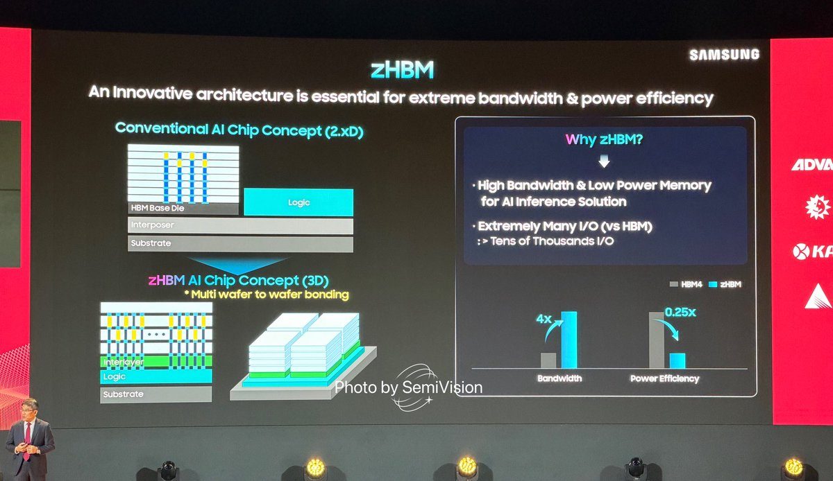
SemiVision 🇹🇼 👁️👁️ on X: "zHBM concept from Samsung #SEMICONKOREA" / X
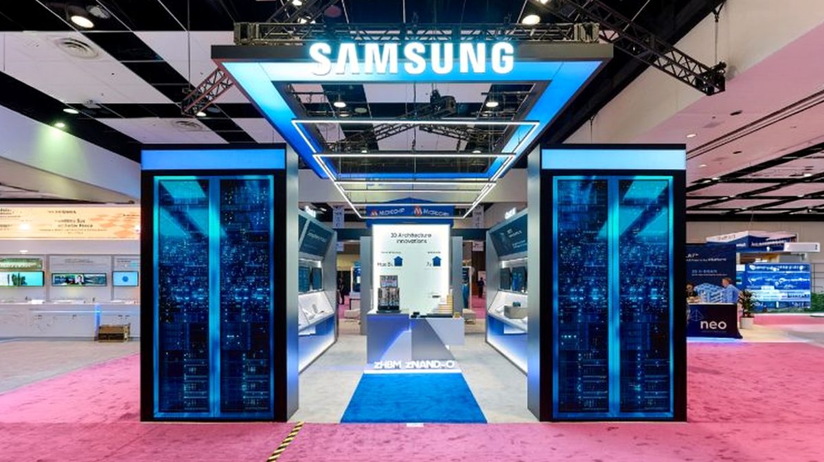
Samsung Unveils Next-Gen 3D-Memory Vision at FMS 2026, Charting the Future of AI Infrastructure | Samsung Semiconductor Global
Hot Chips 2026: Samsung reveals a three-phase HBM roadmap that puts logic and compute inside memory — zHBM ultimately stacks DRAM directly on top of the processor | Tom's Hardware

28 views
8:48
Memory on Top of the GPU: Samsung's zHBM Vision
Semiconductor News / 3-Min Semi with Tai
12.6K views
9:04
Did Samsung Really Just Make Memory 8× Faster?
Cloud Codes

9 views
13:29
Samsung Just Built a 400-Layer Memory Skyscraper for AI
Hidden Tech
Images from Openverse under Creative Commons licenses. Videos from YouTube.
Voices
Curated perspectives — historical figures and your fellow readers.
Play
Exploring all sides of a story is often best achieved with Play.
Most of these play right now — no account needed. Sign up to save scores, keep a streak, and unlock Debate and Predict.
Log in
Sign Up
Higher or Lower
A number from this story, against one from elsewhere in the news — guess which is bigger, then keep the chain going. 5 rounds, 3 strikes; a miss costs a strike and resets your streak.
Example
Anchor
EU tariff revenue
$52B
Big for this kind of number
Mystery
Pentagon AI contract
?
Round 1
Streak: 0
Mystery
?
Keyboard: ↓/L lower · ↑/H higher
0 pts
Best streak: 0 · Rounds: 0
0 points — sign up to put that on the leaderboard.
Now try on this story
Timeline
Samsung stacks memory directly on AI accelerators with zHBM prototype
Order five events from this story, oldest at top. Each in the right slot scores 1 — neighbours within one slot count too. Your previous result — green ✓ for exact slots, yellow ~ for off by one. Cards now in true chronological order.
Loading puzzle…
Tap 💡 Free hint to lock the oldest into slot 1 — that leaves just four to order. Type pills are clues.
0/5
Exact slot
0/5
Within 1
Sign up to save your score and track a streak across stories.
Now try on this story
Connections
Sixteen names from the news. Find the four hidden groups of four. Four mistakes max.
Loading today's puzzle…
0/4 groups
Mistakes
Sign up to keep a daily streak — a new puzzle lands every day.
Now try on this story
Exit debate?
Your progress in this debate will be lost.
How it works
- 1 Two AI personas square off on this story.
- 2 You predict who'll win each round — correct picks earn XP.
- 3 One crossfire question is yours to fire. Pick it carefully.
Couldn't generate a topic
Select Your Champions
Choose one persona for each side of the debate
DEBATE TOPIC
Choose personas with different perspectives for a more dynamic debate.
SIDE A (PRO)
Select debater for this side:
No debate personas available right now.
SIDE B (CON)
Select debater for this side:
No debate personas available right now.
VS
Get ready to make your prediction...
Round of
Claim
Evidence
Stakes
Crossfire Answer
Closing Statement
Claim
Evidence
Stakes
Crossfire Answer
Closing Statement
Your Crossfire Question
Generating arguments...
Who's Got This Round?
Make your prediction before the referee scores
The referee scores both sides on
Correct predictions earn +20 XP
· Press 1 or 2 to pick
Evidence
40%
Logic
30%
Detail
20%
Style
10%
Round Results
Your Pick
Not this time
(%)
Overall Score
/10
Your Pick
Not this time
(%)
Overall Score
/10
Set the Crossfire
Pick the question both personas must answer in the final round
Crafting crossfire questions...
Choosing a question earns +10 XP crossfire bonus
🏆
Total XP Earned
Cred Change
Predictions
Debate Oracle! You called every round!
Sharp Instincts! You know your debaters!
The Coin Flip Strategist! Perfectly balanced!
The Contrarian! Bold predictions!
Inverse Genius! Try betting the opposite next time!
XP Breakdown
Base completion
+20 XP
Rounds played ( rounds x 5 XP)
+ XP
Correct predictions ( correct x 20 XP)
+ XP
Crossfire bonus
+10 XP
Accuracy
%
Prediction History
Round
You picked:
✓
✗
Now try on this story
Keep debating to level up your credibility and unlock achievements
People Involved
Organizations Involved
Samsung Electronics
Semiconductor manufacturer
Developing zHBM, currently shipping HBM4
South Korea's largest semiconductor maker, developing zHBM to stack memory directly on AI accelerators.
SK Hynix
Semiconductor manufacturer
Current HBM market leader, Samsung's main rival
SK hynix leads the HBM market and is advancing interposer technology alongside TSMC.
Taiwan Semiconductor Manufacturing Company (TSMC)
Contract chipmaker
Partner and competitor in advanced packaging
The world's largest contract chipmaker, advancing interposer technology for AI accelerators.
Timeline
February 2026 September 2026
6 events
Latest: 3 days ago
Tap a bar to jump to that date
-
Samsung debuts zHBM prototype
Latest ProductSamsung shows a working zHBM prototype, stacking memory directly on AI accelerators, at proof-of-concept stage.
-
Samsung showcases zHBM at SEMICON Taiwan
AnnouncementSamsung presents the CUBE strategy and zHBM targets: 8x HBM4E performance, 3x power efficiency, 75-90% lower thermal resistance.
-
Hot Chips 2026 details three-phase HBM roadmap
PresentationSamsung's Sangwook Han presents the roadmap from HBM4 base die to zHBM, eliminating the interposer in phase three.
-
Samsung unveils zHBM concept at FMS 2026
AnnouncementSamsung shows the first zHBM concept model at the Future of Memory and Storage conference, alongside zNAND-O.
-
Samsung samples HBM4E to customers
ProductSamsung ships HBM4E samples, with mass production targeted for the following year.
-
Samsung begins HBM4 mass production
ProductSamsung starts shipping HBM4, its current high-bandwidth memory product, built on a 4nm logic base die.
Historical Context
3 moments from history that rhyme with this story — and how they unfolded.
August 2013
Samsung V-NAND (2013)
Samsung introduced V-NAND, the first commercial 3D NAND flash memory, stacking cells vertically instead of shrinking them on a flat plane. The industry had hit scaling limits with planar NAND, and Samsung bet on vertical stacking to keep density growing.
Then
Samsung became the NAND flash leader and held that position for years as rivals scrambled to catch up with 3D stacking.
Now
3D NAND became the industry standard, and Samsung's stacking expertise became a core competitive advantage.
Why this matters now
Samsung is making the same bet with zHBM: vertical stacking to solve a scaling and performance problem. The company explicitly cites its V-NAND and through-silicon via experience as the foundation for zHBM's wafer bonding.
2013-2015
SK hynix HBM debut (2013)
SK hynix developed high-bandwidth memory with AMD, stacking DRAM dies vertically and connecting them with through-silicon vias. HBM was initially seen as a niche product for GPUs, with skeptics questioning its cost and complexity.
Then
HBM found early use in AMD's Fury graphics cards but remained a small market for years.
Now
The AI boom made HBM essential, and SK hynix became the dominant supplier to Nvidia, holding the market lead Samsung now wants to take back.
Why this matters now
zHBM is a similar bet on a new memory architecture that could become essential. The difference: this time Samsung is the one making the radical bet, and SK hynix is the incumbent defending the interposer approach.
July 2015
Intel-Micron 3D XPoint (2015)
Intel and Micron announced 3D XPoint, a new memory technology they claimed was up to 1,000x faster than NAND and 10x denser than DRAM. It was positioned as a revolutionary new class of memory that would bridge the gap between storage and RAM.
Then
3D XPoint shipped as Intel Optane in 2017 but saw limited adoption due to high cost and niche use cases.
Now
Intel discontinued Optane in 2022, and 3D XPoint never achieved mainstream success, a cautionary tale for new memory architectures.
Why this matters now
zHBM faces the same adoption risk: a technically impressive new memory architecture that must prove it can be manufactured at scale and find enough customers to justify the investment.
Sources
(9)Related Stories
SK hynix ships first 12-layer HBM4E samples for AI systems
New Capabilities
Updated Jun 18
First open standard published for high bandwidth flash AI memory
New Capabilities
Updated Aug 4
The race to break AI's memory wall
New Capabilities
Updated May 16
The packaging pivot: why AI's real bottleneck isn't chips—it's putting them together
Built World
Updated May 20
Arm puts neural accelerators inside mobile GPU with CSS for Mobile 2
New Capabilities
Updated Yesterday
Intel's 18A gambit: the chip that could save a semiconductor giant
New Capabilities
Updated May 19